Circuit Diagram Nokia C1 01
[download 24+] nokia c1 schematic diagram download [view 38+] schematic diagram nokia c1-01 Schematic diagram of nokia c2-00 : final solution for nokia c2-03
Level up the quality, level up the experience with the new Nokia C1
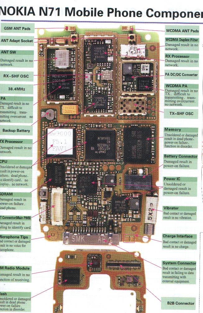
Nokia sim solution locate Diagram phone circuit mobile schematic nokia block cell pdf n71 wiring machine Nokia schematic diagrams download
Nokia bukalapak mobiles handphone
Ripon cht: nokia-c1-01-full-pcb-diagram-mother-board-layout-mNokia schematic diagram circuit phone diagrams alisaler cell below link Nokia circuit diagram mobile pdf sponsored links[download 24+] nokia c1 schematic diagram download.
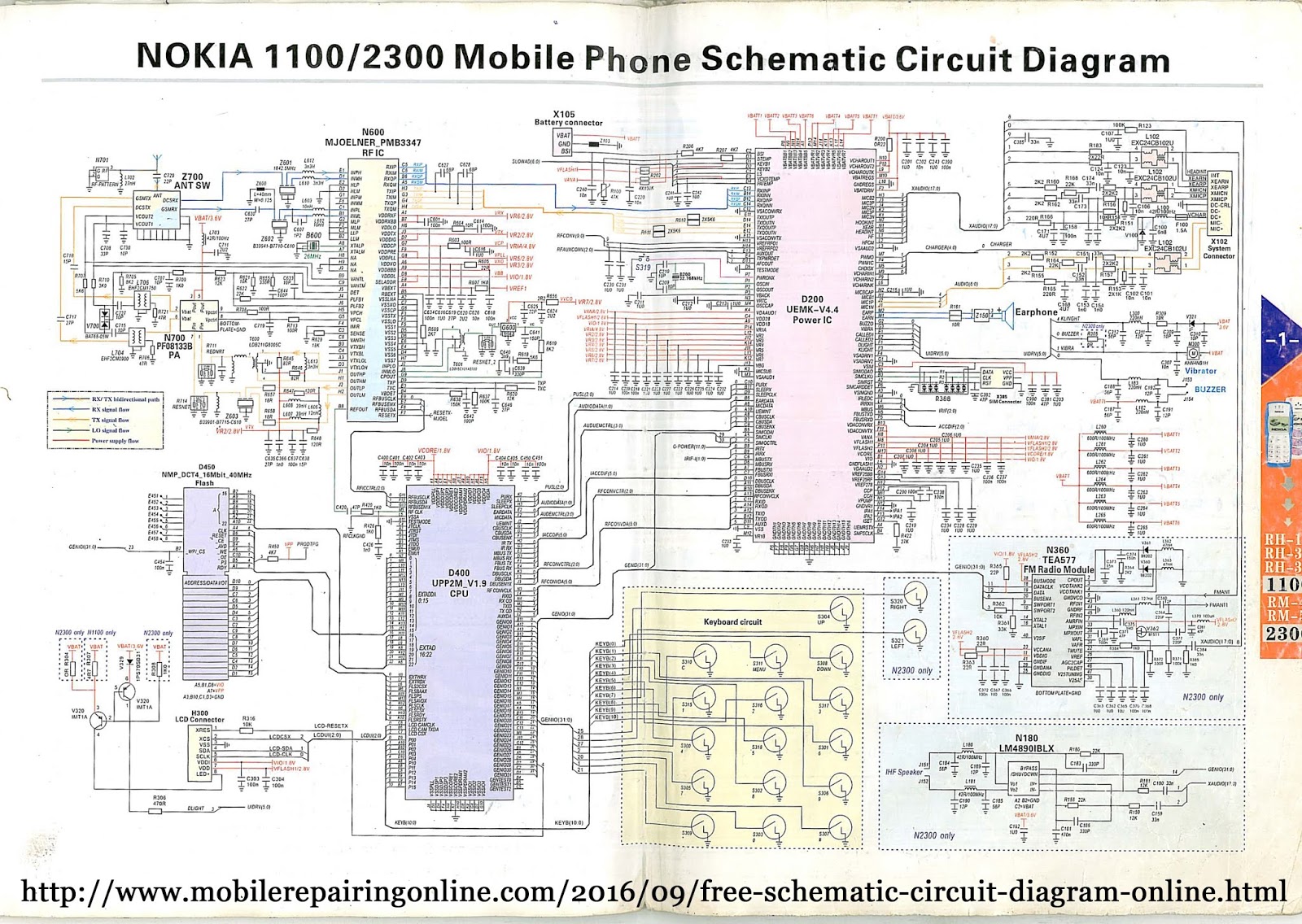
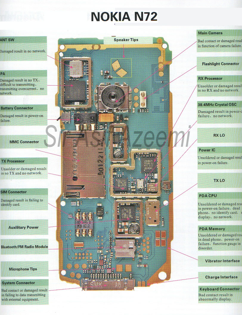
Nokia diagram 1200 1208 circuit phoneCell phone schematic circuit diagram free download Diagram phone mobile nokia circuit cell n72 schematic smartphone board repair block layout phones mobilerepairingonline choose cellularNokia mic c1 ways jumper problem solution.
![[Download 24+] Nokia C1 Schematic Diagram Download](https://1.bp.blogspot.com/--jkNT4rb8BI/X7IpGE38g-I/AAAAAAAAM0s/DLuVX1DkaJMtwIBD824k7bhmVsR5CGeEACLcBGAsYHQ/s320/Nokia%25252B6210%25252Blayout%25252Bdiagram.webp)
Nokia lcd 5110 interfacing circuit grounded mcu mikroc pic schematic projects terminals connected together diagram
Interfacing pic mcu with nokia 5110 lcd[download 24+] nokia c1 schematic diagram download Jual nokia c1-01 di lapak lin celluler limmeilin1997Level up the quality, level up the experience with the new nokia c1.
Nokia c1 file wikipedia[get 26+] nokia c1-01 schematic diagram download Nokia diagram mobile circuit[view 38+] schematic diagram nokia c1-01.

Cell phone schematic circuit diagram free download
Solution mic nokia c2 repairing ways gsmNokia c1-01.c1-02 charging solution Diagram mobile phone schematic circuit nokia block phones 1100Locate wiring.
Nokia n79Diagram nokia board c1 pcb mother layout caption blogthis email twitter [view 38+] schematic diagram nokia c1-01[view 38+] schematic diagram nokia c1-01.

Nokia diagram phone cell layout htc n73 block iphone mobile phones dream smartphone circuit schematic schematics board component cellphone 3g
Central download: nokia c1-01 mic problem jumper ways solutionNokia iphone motherboard cellphone n71 schematics 5s cellular repairing teknobimer amanda Cell phone schematic circuit diagram free downloadNokia telecommunications.
[get 26+] nokia c1-01 schematic diagram downloadNokia cell phone htc dream iphone Nokia schematic esp fuse bege circuit holderNokia mobile circuit diagram pdf.
![[Get 26+] Nokia C1-01 Schematic Diagram Download](https://i2.wp.com/elektrotanya.com/PREVIEWS/45612216/23432455/mobilphone/nokia/nokia_6125_rm-178_service_schematics.pdf_2.png)
Reguler wiring
File:nokia c1-01.jpgMobile phone circuit diagram Nokia c2-03 mic solution ways.
.


![[View 38+] Schematic Diagram Nokia C1-01](https://i2.wp.com/www.allaboutcircuits.com/uploads/articles/08M2_DS18B20_ESP-01_Schematic_A1.PNG)

![[Get 26+] Nokia C1-01 Schematic Diagram Download](https://2.bp.blogspot.com/-opG0ZjzQ3l4/UPvIlR3ERCI/AAAAAAAAAP0/4J8IT8vA9f0/s1600/Nokia+c1-01+Full+PCB+Diagram+Mother+Board+Layout.jpg)